SEMITIP, version 6
Based on versions 1-5 of SEMITIP, written by R. M. Feenstra during 2001 - Feb/2011
Version 6 introduced May/2011.
Introduction
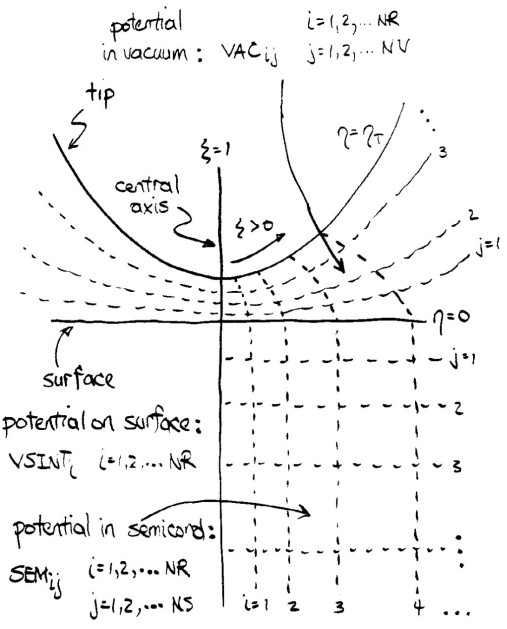
SEMITIP is a Poisson solver specifically designed for problems involving a hyperbolic shaped probe
tip in proximity to a semiconductor. Arbitrary spatial arrangements of surface (or bulk) charges can be specified, the solution for which is obtained using an iterative finite-difference method. The semiconductor is treated in an effective-mass (envelope function) approximation. Tunnel currents are computed using the Bardeen method, with the solution of Schrödinger's equation performed either with a "central axis approximation" in which numerical integration of the equation is performed only the central axis of the problem (an exact solution only for a planar geometry) or using a plane wave expansion over a limited region of space centered around the point on the semiconductor surface opposite the tip apex. Tunnel currents flowing between the tip and the semiconductor sample are output, as are maps of the electrostatic potential, the charge densities, etc.
The sections below provide a general introduction to the SEMITIP V6 package. More detailed information is available in the
SEMITIP V6 Technical Manual.
This software is freely provided for use by any researcher. Users are encouraged to specify the source of the software ("SEMITIP", with reference to the present Website) in their publications. Additional reference can be made, as appropriate, to the various background publications listed at the bottom of this document.
Differences between Versions 1-5 and Version 6
Two technical changes are implemented in version 6. The first is the introduction of a new method for computing derivatives for the variable-spaced grids that are employed in the finite-difference solution for the potential. This method is further described in
Computation of Derivatives for Variable Grid Spacing. A consequence of this change is that, for zero or low doped semiconductors, tip-induced band bending results from version 6 tend to be somewhat larger than those from version 5 or earlier (for moderate or highly doped semiconductor the results are unchanged).
The second change is inclusion of an option to include the image potential in the vacuum (by setting an
indicator at the final line of the fort.9 input file), as described in
Computation of Tunnel Current for Bulk States (including consideration of image potential and field-emission resonances). This option is
presently only implemented in the UnitInt2 program, employing the intcurr routine, although inclusion into other programs which use that routine can easily be accomplished in the future.
Other than these two technical modifications, all other revisions made in version 6 have to do with packaging of the programs and routines, since version 6 allows a much greater range of types of computations than did versions 1-5.
Versions 1-5 of SEMITIP dealt with only a single dimensionality of the problem, namely, 3D with azimuthal symmetry so that only two coordinates (r and z in the semiconductor, or ξ and η in the vacuum) are needed. Versions 1 - 3 had capability for only the computation of electrostatic potential, whereas versions 4 and 5 provided the capability of computing the tunnel current using a "central axis approximation" in which the Schrödinger equation is solved by numerical integration along the central axis of the problem.
For version 6
of SEMITIP, the types of dimensionalities have been increased to include both the planar geometry (1D potential) as well as a fully 3D (including angular dependence) situation. Also, within each case, various geometries in which the specified surface states or bulk doping concentrations vary in different regions of space are allowed. Additionally, the tunnel currents (and quantum states) can be computed not only with the central axis approximation but also with a type of plane wave expansion. With the considerable variation in types of possible computations, it is necessary to revise the naming conventions of the programs to reflect their particular application. This renaming is described below, and additional details are available in the
SEMITIP V6 Technical Manual.
Downloading and Running the Programs
Executable codes together with input files (FORT.9) can be downloaded as directed under the individual program descriptions below. The program is run simply by double-clicking on the executable code, with the FORT.9 file residing in the same directory as the executable code. Output takes the form of a series of ASCII or binary files (FORT.10, FORT.11, ...), which the user then must plot to view the results. Source codes for all programs and routines are also available, as detailed below.
General Aspects of the Programs and Routines
All programs are written in standard FORTRAN. Executable code is provided, constructed using the Gnu gfortran compiler on a Windows platform, although all source codes are also provided so that the programs can be recompiled and run on any platform. Usage of each individual program listed below is described under its own Web page. A given program will consist of a main calling routine and a few user-defined routines for defining certain quantities (such as the distribution of surface states), together with a set of supporting routines that are used by a range of different programs. As a rule, all input to the programs is passed as a list of numbers within a single file (FORT.9), so that the functioning of the program can be completely controlled by editing the numbers within that file. However, array sizes within the program are defined in a PARAMETER statement, so that if they need to be changed then that statement must edited and the program re-compiled and linked. Also, the program employs several user-defined functions such as one to define a protrusion on the end of the probe tip and others to define the energy distribution of surface states and spatial arrangement of both surface charge density and bulk charge density. Default forms of these functions are provided in the supplied programs, and changes to those will also require re-compiling and linking the program. See the
SEMITIP V6 Technical Manual for additional information.
Available Programs and Routines
Programs are named using a character string describing the geometry of the problem and type of current computation, followed by a number giving the dimensionality, followed by a dash and the version of the program. The dimensionality is specified using 1 for a planar geometry (1D potential), 2 for a 3D geometry with azimuthal (angular) symmetry so that only 2 coordinates are used for the potential, and 3 for a fully 3D geometry. The geometry, of the problems refers to the number of different types of regions within the semiconductor (i.e. with different doping concentrations or specified fixed charges densities) or different types of areas on the surface (i.e. with different surface charge densities or specified fixed charge densities) that can be included. The program name "Uni" is used for a uniform semiconductor and "Mult" for a nonuniform semiconductor with multiple regions and/or surface areas. The type of current computation is specified using "Int" for the numerical integration using the central axis approximation, or "Plane" for a plane wave computation. The former corresponds to a computation with planar electrodes, so it is an approximation in 3D situations, but nevertheless it still works well in situations where the potential varies slowly in the radial direction. The plane wave expansion method provides a more general method of computing the current, but because of the significant computational demands of the technique it is only possible to treat a small spatial region around the point on the semiconductor surface opposite the tip apex.
The suite of programs within the SEMITIP package include both general purpose programs, for which all input is specified through the FORT.9 input file or the standard user-defined routines, and special purpose programs, which deal with specific situations or geometries not handled by the general purpose programs. In the descriptions below, a "uniform" semiconductor is one that is homogeneous in terms of computation of an electrostatic potential. That is, the material has constant dielectric constant, doping concentrations, effective masses, band gap, and surface state distributions. However in such a material, spatially varying fixed charge on the surface or in the bulk can still be introduced, which will of course produce a varying electrostatic potential; see
Uni3
for an example (users who plan to investigate fixed charges should also refer to the section on
Specification of Fixed Charge on Surface or in Bulk
in the
SEMITIP V6 Technical Manual). Additionally, shifts of the band edge positions can be introduced after computation of the electrostatic potential, e.g. as would occur by a quantum dot in undoped material, with the resulting spatially varying band structure used for computation of the tunnel current (see
UniPlane3
for an example).
A "nonuniform" semiconductor in the descriptions below is one in which there is a spatial inhomogeneity in the doping concentration, effective masses, band gap, or surface state distributions. In these cases, multiple types of regions in the bulk of the semiconductor and/or multiple types of surface areas are defined, and these are handled appropriately by the finite-difference solution for the potential. However, the grids of these general purpose programs for handling inhomogenous materials are not precisely matched to the boundaries of the different spatial areas or regions in the material, and neither can the programs handle any change in the dielectric constant between the different regions. (Actually, the Mult programs for handling nonuniform semiconductors represent only a modest extension of the Uni programs that handle uniform semiconductors, in that there is a built-in capability for inputting multiple semiconductor regions and/or surface areas and passing those parameters to the routines defining charge densities and band gaps).
Programs that incorporate additional features, such as specialized grids for inhomogeneous geometries, can be developed by extension of the general purpose programs below. An example of one such special purpose program, for handling a thin film of one type of semiconductor on top of another type of semiconductor, is provided by the program
Film2
described below.
General purpose programs:
-
Uni1 -
Potential computations for a uniform semiconductor, in a planar geometry (1D potential).
-
UniInt1 -
Potential computations for a uniform semiconductor, along with computations of tunnel current using numerical integration of Schrödinger's equation, in a planar geometry (the potential is 1D, in the z direction, but the current is computed with full inclusion of quantum states traveling in the x and y directions as well).
-
UniIntSC1 -
Potential computations for a uniform semiconductor, along with computations of tunnel current using numerical integration of Schrödinger's equation, in a planar geometry. The potential is computed self-consistently, using the quantum states from the solution to Schrödinger's equation, so that e.g. inversion or accumulation layer states are computed exactly.
-
Mult1 -
Potential computations for a nonuniform semiconductor, in a planar geometry (1D potential).
-
MultInt1 -
Potential computations for a nonuniform semiconductor, along with computations of tunnel current using numerical integration of Schrödinger's equation, in a planar geometry (the potential is 1D, in the z direction, but the current is computed with full inclusion of quantum states traveling in the x and y directions as well).
-
Uni2 -
Potential computations for a uniform semiconductor, with a hyperbolic shaped probe tip, in a 3D geometry with azimuthal symmetry.
-
UniInt2 -
Potential computations for a uniform semiconductor, along with computations of tunnel current using numerical integration of Schrödinger's equation along the central axis, in a 3D geometry with azimuthal symmetry.
-
UniIntSC2 -
Potential computations for a uniform semiconductor, along with computations of tunnel current using numerical integration of Schrödinger's equation along the central axis. The potential is computed self-consistently, using the quantum states from the solution to Schrödinger's equation that are computed at a series of different radial distances from the central axis.
-
Mult2 -
Potential computations for a nonuniform semiconductor, with a hyperbolic shaped probe tip, in a 3D geometry with azimuthal symmetry.
-
MultInt2 -
Potential computations for a nonuniform semiconductor, along with computations of tunnel current using numerical integration of Schrödinger's equation along the central axis, in a 3D geometry with azimuthal symmetry.
-
Uni3 -
Potential computations for a uniform semiconductor, in a fully 3D geometry.
-
UniInt3 -
Potential computations for a uniform semiconductor, along with computations of tunnel current using numerical integration of Schrödinger's equation along the central axis, in a fully 3D geometry.
-
UniPlane3 -
Potential computations for a uniform semiconductor, in a fully 3D geometry. The tunnel current is computed using a plane wave expansion method. The plane wave method necessarily includes only a relatively small spatial region centered about the point on the semiconductor surface opposite the apex of the probe tip, but the results nevertheless provide a good approximation in many cases. A localized potential such as occurs e.g. for a quantum dot can be included in the computation of the tunnel current.
-
Mult3 -
Potential computations for a nonuniform semiconductor, in a fully 3D geometry.
-
MultInt3 -
Potential computations for a nonuniform semiconductor, along with computations of tunnel current using numerical integration of Schrödinger's equation along the central axis, in a fully 3D geometry.
-
MultPlane3 -
Potential computations for a nonuniform semiconductor, in a fully 3D geometry. The tunnel current is computed using a plane wave expansion method. The plane wave method necessarily includes only a relatively small spatial region centered about the point on the semiconductor surface opposite the apex of the probe tip, but the results nevertheless provide a good approximation in many cases. A localized potential such as occurs e.g. for a quantum dot can be included in the computation of the tunnel current. (The nonuniform aspect of the semiconductor is intended to handle situations that affect the electrostatic potential, e.g. due to differently doped layers in a semiconductor heterostructure. In contrast, the region of localized potential opposite the probe tip is introduced as something that affects the tunnel current, but not the electrostatic potential itself).
Special purpose programs:
-
Film2 -
Potential computations for a thin film of one type of semiconductor on top of another type of semiconductor, with a hyperbolic shaped probe tip, in a 3D geometry with azimuthal symmetry. Surface charge density from a user specified distribution of surface states can be included, and interface states between the semiconductor film and substrate can also be included.
Supporting Routines:
Supporting routines for the programs are labeled similarly to the programs, with a character string describing the purpose of the routine followed by a number (if needed) giving the dimensionality that it applies to. The supporting routines currently available are:
-
BoundWell3E -
Routine for forming plane wave basis states for conduction band (including extended states).
-
BoundWell3V -
Routine for forming plane wave basis states for valence band.
-
contr2 -
Routine for producing contours plots of the potential, for a 3D potential with azimuthal symmetry.
-
contr3 -
Routine for producing contours plots of the potential, for a 3D potential, at a specified azimuthal angle.
-
dgsect -
General purpose double precision Golden Section search routine, used in forming plane wave basis.
-
GetCurr -
Used for plane wave solution of tunnel current, to sum up states.
-
gsect -
General purpose Golden Section search routine, for dealing with nonlinear aspects of the solution for the potential.
-
intcurr -
Routine for performing numerical integration of Schrödinger equation, along a given potential curve (supplied by potexpand2 or potexpand3). The wavefunctions thus obtained are used for computing tunnel currents as well as for computing charge densities as needed for self-consistent solutions of Poisson's and Schrödinger's equations.
-
planecurr3 -
Routines for performing the eigenvalue solution of Schrödinger's equation with a plane wave basis.
-
PlotGray -
General purpose routine for producing gray scale plots of 2D functions (used for plotting charge densities or potential maps).
-
potcut2 -
Routine for taking a cut of the potential along the the central axis (r=0), using the potential array from semitip2.
-
potcut3 -
Takes a cut of the potential along the the central axis (r=0), using the potential array from semitip3.
-
potexpand -
Expands the potential curves produced by potcut2 or potcut3, to produce a point-to-point resolution of the curves that is suitable for numerical integration.
-
potperiod3 -
Expands the potential evaluated on the grid from semitip3 into a finer grid with uniform spacing, as needed by planecurr3.
-
rseispackALL -
EISPACK routines for solving the eigenvalue problem of a real, symmetric, double precision matrix.
-
semirho -
Set of routines for computing semiconductor charge densities, for a uniform (homogeneous) semiconductor.
-
semirhomult -
Set of routines for computing semiconductor charge densities, for an inhomogeneous semiconductor with multiple regions with different types of charge densities.
-
semitip1 -
Finite-difference routine for obtaining the solution of Poisson's equation, in 1D.
-
semitip2 -
Finite-difference routine for obtaining the solution of Poisson's equation, in 3D with azimuthal symmetry.
-
semitip3 -
Finite-difference routine for obtaining the solution of Poisson's equation, in 3D without azimuthal symmetry.
-
surfrho -
Set of routines for handling charge densities on a uniform (homogeneous) semiconductor surface.
-
surfrhomult -
Set of routines for handling charge densities on an inhomogeneous semiconductor surface with multiple areas having different types of charge densities.
Theory
The physical concepts and computational techniques that forms the basis for the programs are described in Refs. [1]-[6] listed below and in the
SEMITIP V6 Technical Manual. Additional information on some of the methods is contained in:
Revisions and Bugs
Revisions to the programs and routines are labeled as described above, with brief comments regarding the revisions provided in the documentation for each program and also within the source code. Among the major supporting routines, the semitip2.f routine (finite-element Poisson solver, for 3D symmetry with azimuthal symmetry) is the most well established one, having been used and tested for many years. The semitip3.f Poisson solver has similarly been used for many years, but its current form was a complete rewrite of prior versions, so residual bugs are possible. For tunnel current computations, intcurr.f has also been used and tested for many years, and is in its nearly original form. But, this code has not yet been updated or "packaged" in the same form as semitip2.f. The same comments apply to planecurr3.f.
A significant error in one specific portion of the package was discovered, and corrected, in Oct. 2015. This error was in regard to the surface state densities which can be input to the package. For convenience to the user, two separate distributions of surface states were allowed to be input, each with their own values of density, charge neutrality level, etc. If nonzero values were input for both of the distributions, then the program was supposed to combine these two distributions into a resultant distribution. This process would also yield a resultant charge neutrality level for the combined distribution. However, the procedure for producing this combined distribution and combined charge neutrality level was found to be in error, i.e. in routines surfrho-6.1.f and surfrhomult-6.1.f and earlier. The correct procedure is implemented in routines surfrho-6.2.f and surfrhomult-6.2.f and later. For more details, see
Surface Charge arising from a distribution of Surface States
Users are welcome to contact Randall Feenstra (feenstra@cmu.edu) with notification of any bugs that might be found in the programs and routines. Also, suggestions for improvement to the documentation, including minor corrections, are always welcome.
Validation
The Poisson solver (semitip2) has been validated by taking its computed potential and charge densities, and using the method of images to compute the potential on the probe tip, as described in Ref. [2]. Good agreement is found with the originally specified tip potential (although as discussed in
example 5 of Uni2.f,
this agreement does not necessarily prove the absolute correctness of the solution for the potential). Additionally, the computed potential agree well with the actual potential for situations where the potential has a simple known form; see
example 2 of Uni1.f and
example 6 of Uni2.f.
Separately, for the two routines that implement different methods of solution of Schrödinger's equation (intcurr and planecurr), they both involve approximations but quite different ones. For an appropriate geometry, results from both methods are in good agreement with each other, as described in Ref. [6] and further discussed in
example 1 of UniPlane3.f.
Of course, agreement of the other routines (semitip3, etc.) with these validated routines, for appropriate limiting cases, has been carefully checked. Nevertheless, these positive test results certainly do not guarantee correctness of the code for every possible situation. Users are encouraged to report any apparent discrepencies in the results to Randall Feenstra (feenstra@cmu.edu).
Acknowledgements
Development of SEMITIP began when the author was working in Berlin during 2001 on a Fellowship from the A. v. Humboldt Foundation. Extension of the code over the subsequent years was supported by the U.S. National Science Foundation. The support of these organizations is gratefully acknowledged.
References
1. R. M. Feenstra, Electrostatic Potential for a Hyperbolic Probe Tip near a Semiconductor, J. Vac. Sci. Technol. B 21, 2080 (2003). For preprint, see
http://www.cmu.edu/physics/stm/publ/52/.
2. R. M. Feenstra, S. Gaan, G. Meyer, and K. H. Rieder, Low-temperature tunneling spectroscopy of Ge(111)c(2x8) surfaces, Phys. Rev. B 71, 125316 (2005). For preprint, see
http://www.cmu.edu/physics/stm/publ/65/.
3. R. M. Feenstra, Y. Dong, M. P. Semtsiv, and W. T. Masselink, Influence of Tip-induced Band Bending on Tunneling Spectra of Semiconductor Surfaces, Nanotechnology 18, 044015 (2007). For preprint, see
http://www.cmu.edu/physics/stm/publ/74/.
4. Y. Dong, R. M. Feenstra, M. P. Semtsiv and W. T. Masselink, Band Offsets of InGaP/GaAs Heterojunctions by Scanning Tunneling Spectroscopy, J. Appl. Phys. 103, 073704 (2008).
For preprint, see
http://www.cmu.edu/physics/stm/publ/79/.
5. N. Ishida, K. Sueoka, and R. M. Feenstra, Influence of surface states on tunneling spectra of n-type GaAs(110) surfaces, Phys. Rev. B 80 075320 (2009).
For reprint, see
http://www.cmu.edu/physics/stm/publ/85/.
6. S. Gaan, G. He, R. M. Feenstra, J. Walker, and E. Towe, Size, shape, composition, and electronic properties of InAs/GaAs quantum dots by scanning tunneling microscopy and spectroscopy, J. Appl. Phys. 108, 114315 (2010). For preprint, see
http://www.cmu.edu/physics/stm/publ/93/.