FPGA– (pronounced FPGA-minus-minus) is a custom digital integrated circuit designed from scratch and taped out as part of the Carnegie Mellon University course 18-725: Advanced Digital Integrated Circuit Design in Spring 2024, with subsequent physical silicon validation and characterization completed in the follow-up course 18-726: Projects in Integrated Circuit Design: First Silicon in Fall 2024. The project covers the complete digital IC lifecycle, starting from architecture definition and Verilog RTL implementation, moving to CAD toolchain integration, and concluding with cell synthesis, physical place-and-route (PAR), Layout-Versus-Schematic (LVS) / Design Rule Check (DRC) signoff, and hands-on lab validation of the returned ASIC.
Architectural Overview & Block Design
The main objective of FPGA– was to build a functional, synthesizable FPGA fabric capable of running user bitstreams. The microarchitecture consists of three primary components: Configurable Logic Blocks (CLBs), configurable routing channels (Connection and Switch Boxes), and configurable I/O blocks.
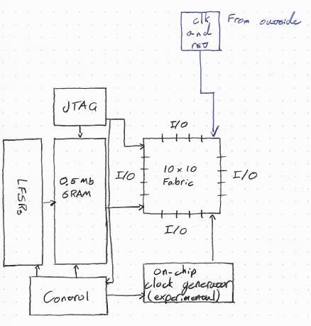
Figure 1: The block diagram and system partitioning for the FPGA-- architecture, illustrating the CLB tile, Connection Boxes (CB), Switch Boxes (SB), and JTAG control interfaces.
1. Configurable Logic Block (CLB)
Each logic tile contains a CLB consisting of:
- Fracturable 3-LUTs: Two 3-input Look-Up Tables (LUTs) that can operate independently or be combined to implement larger functions.
- Flip-Flop: A dedicated state element for sequential logic.
- Carry Chain: An optimized carry-propagation line to accelerate adders and arithmetic blocks.
2. Configurable Routing
The routing architecture handles local and global signal routing:
- Connection Boxes (CB): Interface the inputs and outputs of the CLB with the horizontal and vertical routing channels.
- Switch Boxes (SB): Implement routing track intersections, routing signals across rows and columns.
3. External Interface & Programming Flow
- JTAG Interface: Serves as the primary programming and debug interface, running on a 10 MHz clock.
- Scan-Chain Configuration: All configuration and state elements across the fabric are linked into a single, continuous scan-chain. Dedicated JTAG instructions are implemented to enable separate access to the fabric scan-chain, on-chip data buffers, and the control unit.
- Offline Data Buffers: The fabric runs offline. Inputs are preloaded into on-chip buffers via JTAG, and outputs are read back.
- Built-in LFSRs: Linear Feedback Shift Registers are integrated to generate pseudo-random data for offline power and toggle-rate analysis.
Technical Specifications
The table below contrasts the ambitious targets defined in our initial project proposal against the actual parameters implemented for the final tapeout:
| Parameter | Proposal Target | Final Tapeout Implementation |
|---|---|---|
| Silicon Area | 1.0 mm2 | ~0.5 mm2 |
| Fabric Grid Size | 10 $\times$ 10 CLBs | 4 $\times$ 4 CLBs |
| Logic Element Capacity | 200 3-LUTs, 100 FF | 32 3-LUTs, 16 FF |
| Internal Memory | 0.5 Mb SRAM | Simplified SRAM buffer registers |
| Target Frequency | 250 MHz | 250 MHz |
| Operating Power | 100 mW | ~15 mW (scaled) |
| GPIO Interface | ~16 Pins | 16 Pins (with extra I/O selection modes) |
| Programming Interface | JTAG (10 MHz) | JTAG (10 MHz) + Scan-Chain |
CAD Toolchain & VTR Integration
Mapping user circuits to a custom FPGA fabric requires a specialized CAD toolchain. We planned to integrate our fabric with the open-source VTR (Verilog-to-Routing) toolchain:
- Synthesis & Mapping: Standard Verilog designs are synthesized and mapped to our custom fracturable 3-LUT architecture.
- Place and Route: VTR places and routes the design onto the target grid configuration.
- Bitstream Generation: A custom script converts the routing and LUT configuration output from VTR into a binary bitstream loadable via JTAG.
Because a standard FPGA is highly regular, it is highly suited for a bottom-up physical design flow. However, standard ASIC CAD tools often struggle with the recursive structures of configurable fabrics and the combinational paths introduced by the switches. We had to take the place-and-route constraints into our own hands, explicitly instructing the CAD tools on how to floorplan, place, and route the individual tiles to achieve a clean layout.
The Design Journey & Mid-Semester Pivot
Designing a chip in a single semester is an exercise in managing complexity and adapting to tight deadlines. Our team went through five distinct design iterations before reaching tapeout.
- DR1 (Design Review 1): Initial $10 \times 10$ fabric designed using custom hand layouts.
- ADR1 (Apple Design Review 1): Attempted an ambitious $30 \times 30$ full-custom layout.
- DR2 (Design Review 2): Transitioned to a synthesized $20 \times 20$ fabric to automate the layout.
- ADR2 (Apple Design Review 2): Scaled down to a $4 \times 4$ synthesized fabric to address routing congestion and tool flow issues.
- Tapeout: Final $4 \times 4$ layout utilizing the ADR2 architecture with optimized I/O pad rings and an extra bidirectional I/O mode.
The Mid-Semester Pivot: Halfway through the semester, we hit major blocking issues with routing congestion and CAD tools. To meet the tapeout deadline, we made the difficult but necessary decision to discard a significant portion of our prior layout efforts. We started almost from scratch, preserving only the Connection Box (CB) and Switch Box (SB) layout blocks, and scaled the fabric down to $4 \times 4$. This pivot cleared the blockages and guaranteed a successful tapeout.
Physical Design: P&R, LVS, and DRC
The backend physical design phase was also a challenging part of the project. Translating the synthesizable Verilog RTL into clean silicon layout geometries required multiple iterations.
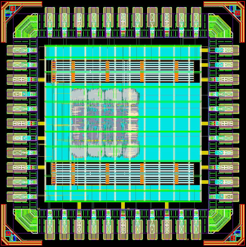
Figure 3: The final physical chip layout of the $4 \times 4$ FPGA-- fabric.
Layout & Routing Verification
During the Physical Action Review, we encountered significant Layout-Versus-Schematic (LVS) mismatches and Design Rule Check (DRC) violations. LVS errors, which often stem from subtle bulk connection mismatches or layout generator bugs, were the most difficult to isolate.
With assistance from the awesome course staff (Prof. Ken Mai and Prof. Prashanth Mohan), we debugged the auto-generated layout blocks, verified power grid connectivity, and performed manual cell alignments. The final week of the class was dedicated entirely to DRC cleanup, ensuring that metal densities, spacing rules, and antenna effects conformed to the foundry requirements.
Silicon Validation & 18-726 Testing Results
To validate the manufactured chip, we designed a custom PCB and built a laboratory test bench to interface with the silicon. This testing environment allowed us to program the FPGA fabric, run test vectors, and measure performance.
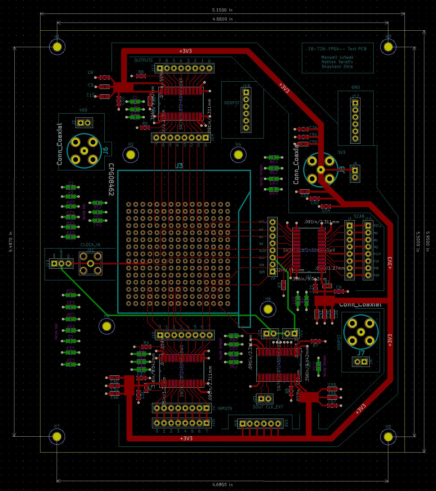
Figure 4: Custom double-sided test PCB designed for the FPGA-- chip validation.
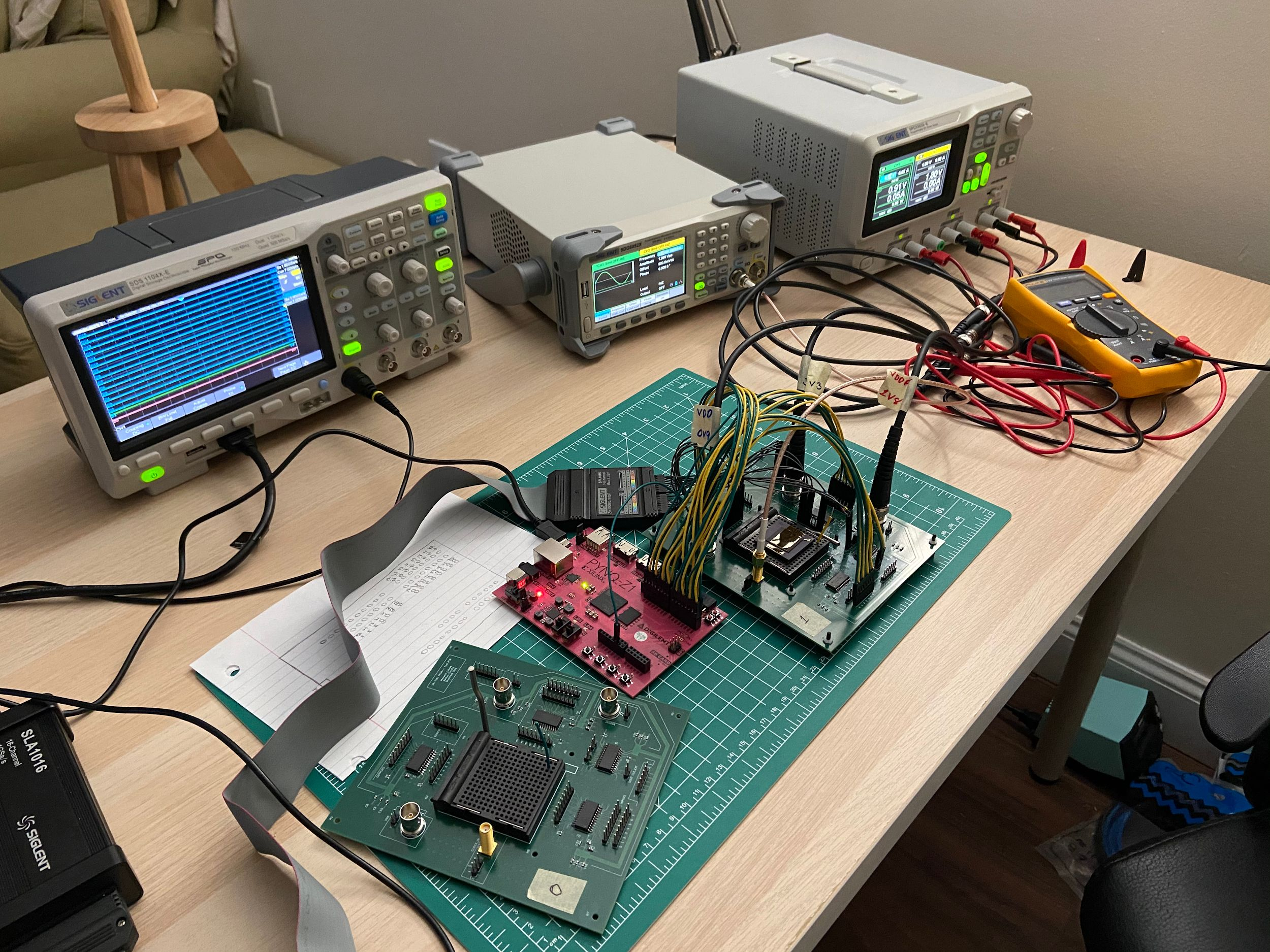
Figure 5: Laboratory test setup including the power supplies, oscilloscope, signal generators, and logic analyzer hooked up to our custom validation board.
Functional Verification
We verified the physical silicon using a suite of custom test bitstreams designed to exercise different aspects of the fabric’s logic and routing. These test designs included simple constant outputs, combinational paths, multi-cycle sequential delays, and arithmetic adders.
The fabric’s logic blocks and configurable routing channels were validated as fully operational, with the clock tree successfully distributing signals up to 500 MHz for sequential test cases. We also mapped the fabric’s operational limits by sweeping the core voltage and frequency, confirming stable routing functionality across a wide voltage range down to 0.60V at lower frequencies.
Power Analysis
- Simulated Core Power: 4.9 mW (post-layout extraction)
- Measured Board-Level Power: 45.5 mW
Our validation measurements showed that total power consumption was heavily dominated by board-level parasitics and active peripheral components on the custom PCB. Because dynamic core power was extremely low, toggling the chip’s internal clock tree had no measurable impact on the total current draw, indicating that core dynamic power was successfully minimized.
Retrospective & Key Takeaways
The retrospective of the FPGA– design process yielded several valuable lessons for future silicon projects:
- RTL Readiness: If you do not have verified RTL in hand at the very start of the semester, the microarchitecture must be kept as simple as possible.
- Scalable Infrastructure: Always build the RTL, generators, and testing benches to be parameterizable. This makes scaling down (e.g., from 20 $\times$ 20 to 4 $\times$ 4) a matter of changing a configuration parameter rather than rewriting code.
- Backup Plans & Deadlines: Always define hard deadlines to switch to backup architectures. We would not have met the tapeout deadline without our pivot after Spring Break.
- Parallel Tasks: Avoid serializing critical design tasks on a single teammate. Parallelizing RTL development, CAD toolchain scripting, and physical design reviews kept the project moving forward.
Team
This chip was co-developed and taped out by:
- Hailang Liou
- Max Lutwak
- Shashank Obla
- Nathan Serafin