Click here for input/output files for Example 3
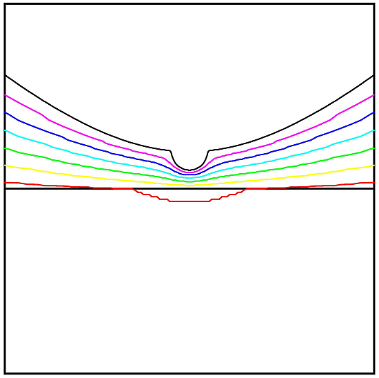
We illustrate the effect of a hemispherical protrusion on the end of the probe tip, for the case of n-type GaAs(110) with a sample bias voltage is 1.0 V and contact potential of 0.0 eV (same parameters as Example 1 except for the presence of the protrusion). Contour lines for the potential from FORT.20 - FORT.26 are shown below, plotted over a horizontal distance of 10 nm and a vertical distance of 10 nm.
It should be noted that inclusion of a probe tip protrusion can lead to rather finely spaced grids for the solution of the electrostatic potential, which in turn could possibly lead to problems in the solution for tunnel current. To date, solutions for the tunnel current when a protrusion is present have not been thoroughly investigated. In most practical problems involving comparison of experimental STM/S data to SEMITIP simulations, it has been found that a protrusion is not needed, since the effect of a protrusion can be equivalently achieved simply by a small change in the overall radius-of-curvation of the hyperbolic tip.