Return
to
Suter
Home
This work is supported by the MRSEC program of the National
Science Foundation under
Award Number DMR-0520425, the NSF Metals program under Award Number
DMR-0805100 and the Department of Energy Basic Energy Sciences under
award DESC0002001. Use of the Advanced Photon Source is
supported by the U. S. Department of Energy Office
of Basic Energy Sciences, under Contract No. DE-AC02-06CH11357. We also
use the computational resources of the NSF TeraGrid.
High Energy X-ray Diffraction Microscopy
(HEDM):
Observing microstructure evolution inside of bulk materials
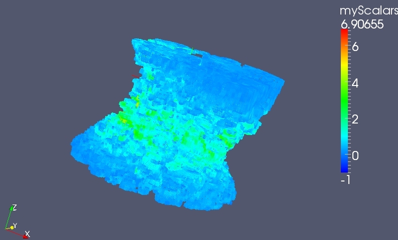
3D representation of local misorientations in a copper wire that has
undergone light tensile strain (reference 3, below).
|
Table
of
Contents (modified November 2010)
- Recent and forthcoming publications
- Technique summary and schematic
- Apparatus at the Advaned Photon Source
- Examples of reconstructions (old)
- Overview
Return to top
Recent and forthcoming publications
- Grain Growth in Pure Nickel in
an Ensemble of 2500 Grains, S.F. Li, C.M. Hefferan, J. Lind, R.
Pokharel, U.
Lienert, A.D. Rollett, and R.M. Suter, in preparation.
- In-situ Observation of Grain
and Sub-grain Response to Tensile Strain in Copper Wires,
S.F.
Li,
J. Lind, C.M. Hefferan, R. Pokharel, U. Lienert, A.D. Rollett,
and R.M. Suter, in preparation.
- Grain Boundary Character
Statistics in Well Ordered Metallic Polycrystals from High Energy X-ray
Diffraction Microscopy, S.F. Li, C.M. Hefferan, J. Lind, U.
Lienert, A.D. Rollett, R.M. Suter, in preparation.
- Combined Microstructure Mapping
and Absorption Tomography Using a Single Crystal Attenuator, P.
Kenesie, A. Khounsary, U. Lienert, J. Lind, S.F. Li, C.M. Hefferan,
R.M. Suter, in preparation.
- Stored Energy Reduction in the
Annealing of High Purity Aluminum Observed with High Energy X-ray
Diffraction Microscopy, S.F. Li, J. Lind, C.M.
Hefferan, U. Lienert, A.D. Rollett, and R.M. Suter, in
preparation.
- High Energy X-ray Diffraction
Microscopy Microstructure Mapping: Current State-of-the-Art,
S.F. Li, J. Lind, C.M. Hefferan, U. Lienert, R.M. Suter, in preparation.
- High-Energy Diffraction
Microscopy at the Advanced Photon Source, U. Lienert, S.F.
Li,
C.M. Hefferan, J. Lind, R.M. Suter, J.V. Bernier, N.R. Barton, C.
Brandes, M.J. Mills, M.P. Miller, B. Jakobsen, and W. Pantleon,
Journal of Materials, July 2011.
- Microstructural
Characterization
and
Evolution
in
3D, S.R. Wilson, C.M. Hefferan,
S.F. Li, J. Lind, R.M. Suter and A.D. Rollett, Risoe 2010 Symposium
proceedings, Challenges in materials
science and possibilities in 3D and 4D characterization techniques,
p.
201,
N.
Hansen,
D.
Juul
Jensen,
S.F.
Nielsen,
H.F. Poulsen, and B.
Ralph, editors (2010).
- 3DXRD
at
the
Advanced
Photon
Source:
Orientation Mapping and Deformation
Studies, U. Lienert, M.C. Brandes, J.V. Bernier, M.J. Mills, M.P.
Miller, S.F. Li, C.M. Hefferan, J. Lind, R.M. Suter, Risoe 2010
Symposium proceedings, Challenges in
materials science and possibilities in 3D and 4D characterization
techniques, p. 59, N. Hansen, D. Juul Jensen, S.F. Nielsen, H.F.
Poulsen, and B. Ralph, editors (2010).
- Tests
of
Microstructure
Reconstruction
by
Forward
Modeling
of
HEDM
Data,
C.M. Hefferan, S.F. Li, J. Lind, and R.M. Suter, Journal of Powder
Diffraction, 25, 132-137
(2010).
- Statistics
of
High
Purity
Nickel
Microstructure
From High Energy
X-ray Diffraction Microscopy, C.M. Hefferan, S.F. Li, J.
Lind, U.
Lienert,
A.D. Rollett, P. Wynblatt, R.M. Suter, Computers, Materials and
Continua, 14, 209-219 (2009).
-
Probing
Microstructure
Dynamics
With
X-ray
Diffraction
Microscopy, R.M.
Suter, C.M. Hefferan, S.F. Li, D. Hennessy, C. Xiao, U.
Lienert, B. Tieman, J. Eng. Mater.
Technol., 130, 021007 (2008);
proceedings of
the Materials Processing
Defects-5
conference, Cornell University, July 2007).
-
3-Dimensional
Characterization of Polycrystalline Bulk Materials Using High-Energy
Synchrotron Radiation, U.
Lienert,
J.
Almer,
B.
Jakobsen,
W.
Pantleon,
H.F.
Poulsen,
D.
Hennessy,
C.
Xiao, and R.M. Suter, Materials Science
Forum 539-543, 2353-2358
(2007).
- Forward
Modeling Method for Microstructure Reconstruction Using X-ray
Diffraction
Microscopy: Single Crystal Verification, R.M. Suter, D.
Hennessy, C. Xiao, U. Lienert. Reviews
of Scientific
Instruments, 77, 123905
(2006).
-
Tracking: a
method for structural characterization of grains in powders or
polycrystals, E.M. Laurdisen, S. Schmidt, R.M. Suter, and
H.F.
Poulsen, J. Appl. Cryst., 34, 744-750 (2001).
-
Three-dimensional
maps
of
grain
boundaries
and
the
stress
state
of
individual
grains
in
polycrystals and powders, H.F. Poulsen, S.F. Nielsen, E.M.
Lauridsen, S. Schmidt, R.M. Suter, U. Lienert, L. Margulies, T.
Lorentzen, and D. Juul Jensen, J. Appl. Cryst., 34,
751-756 (2001).
- Future Trends:
Texture Analysis for Structure-Sensitive Properties, B.L. Adams, D. Juul
Jensen, H.F. Poulsen, and R. Suter, Materials
Science Forum, 273-275, 29-40
(1998).
Return to top
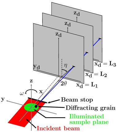
Schematic and Outline of the Technique
- Monochromatic high energy x-rays (energies 50 - 100 keV)
are focused in the vertical direction to form a line-focused beam
roughly 1 -2 microns high and about 1.3mm wide (red).
- This beam illuminates a thin planar section of the sample (green).
- Bragg spots (black) from individual grains are imaged on a CCD
detector (gray); spots have the shape of the illuminated grain cross
section projected onto the detector plane at the scattering angles 2q and f.
- Measuring a set of spots at multiple sample-to-detector distances
yields the path of the diffracted beam and, by inversion, the position
of
the diffracting grain.
- Step-wise measurements over a range of sample orientations, w,
yield multiple spots from each grain; this implies complete
crystallographic orientation information and projected images of each
grain from multiple points of view
|
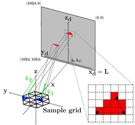
|
- After image processing, our analysis code performs a simulation
of the entire measurement and microstructure. The sample space is
gridded (above right) and the crystallographic orientation in
each grid element (or voxel) is adjusted to optimize the overlap
of simulated Bragg scattering with the experimental data. The search
algorithm works on each voxel independently making parallelization of
the code straightforward.
Return
to
top
Apparatus at APS beamline 1-ID
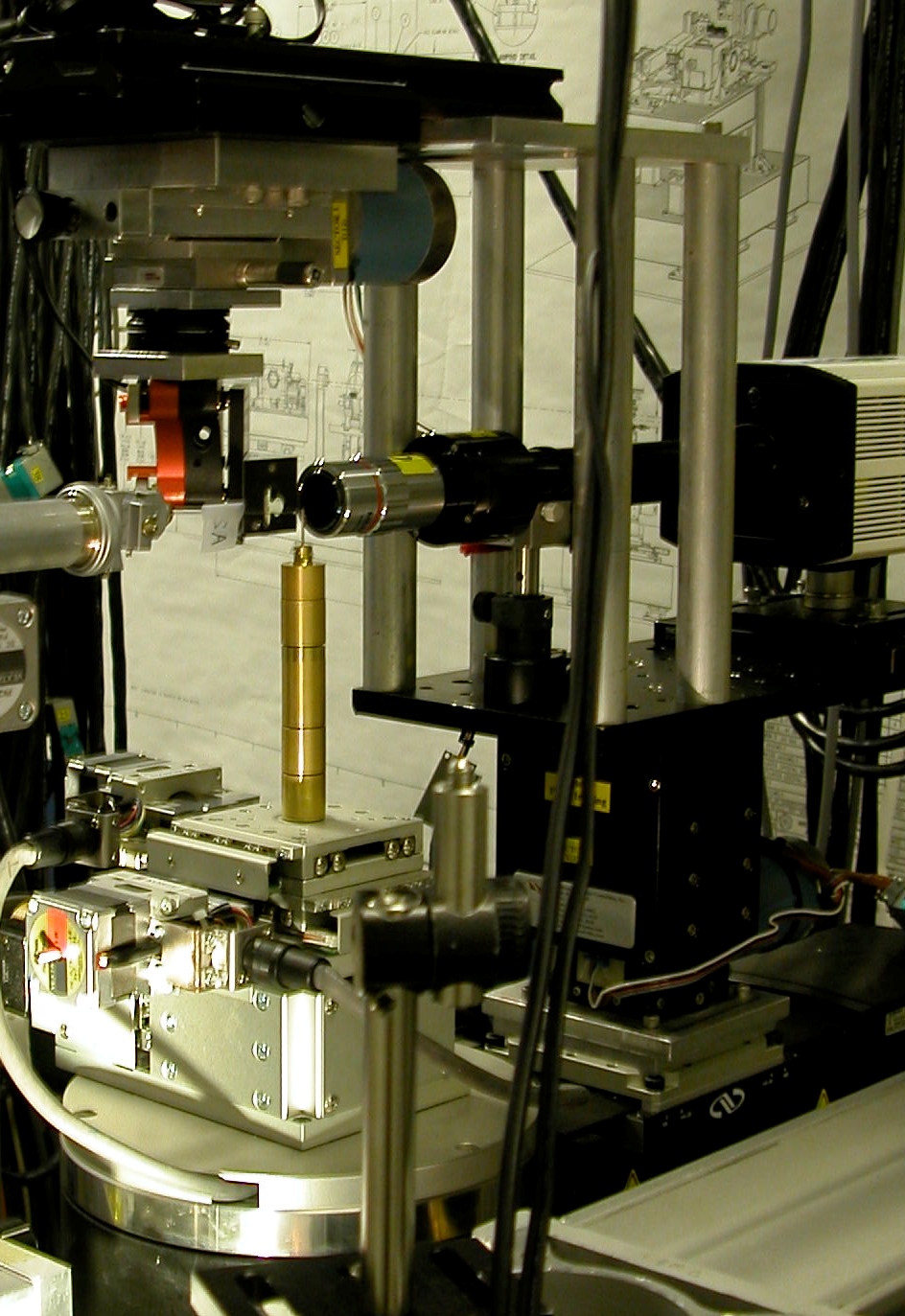
|
Sample
stage
at
1-IDB.
- CCD camera lens collects scintillation light off a 45
degree mirror.
- LuAG scintillator and 45 degree mirror holder
- Beam attenuator (holder extends from left)
- Sample (above brass offset)
- XYZ translations stage
- Precitech air-bearing rotation stage
|
|
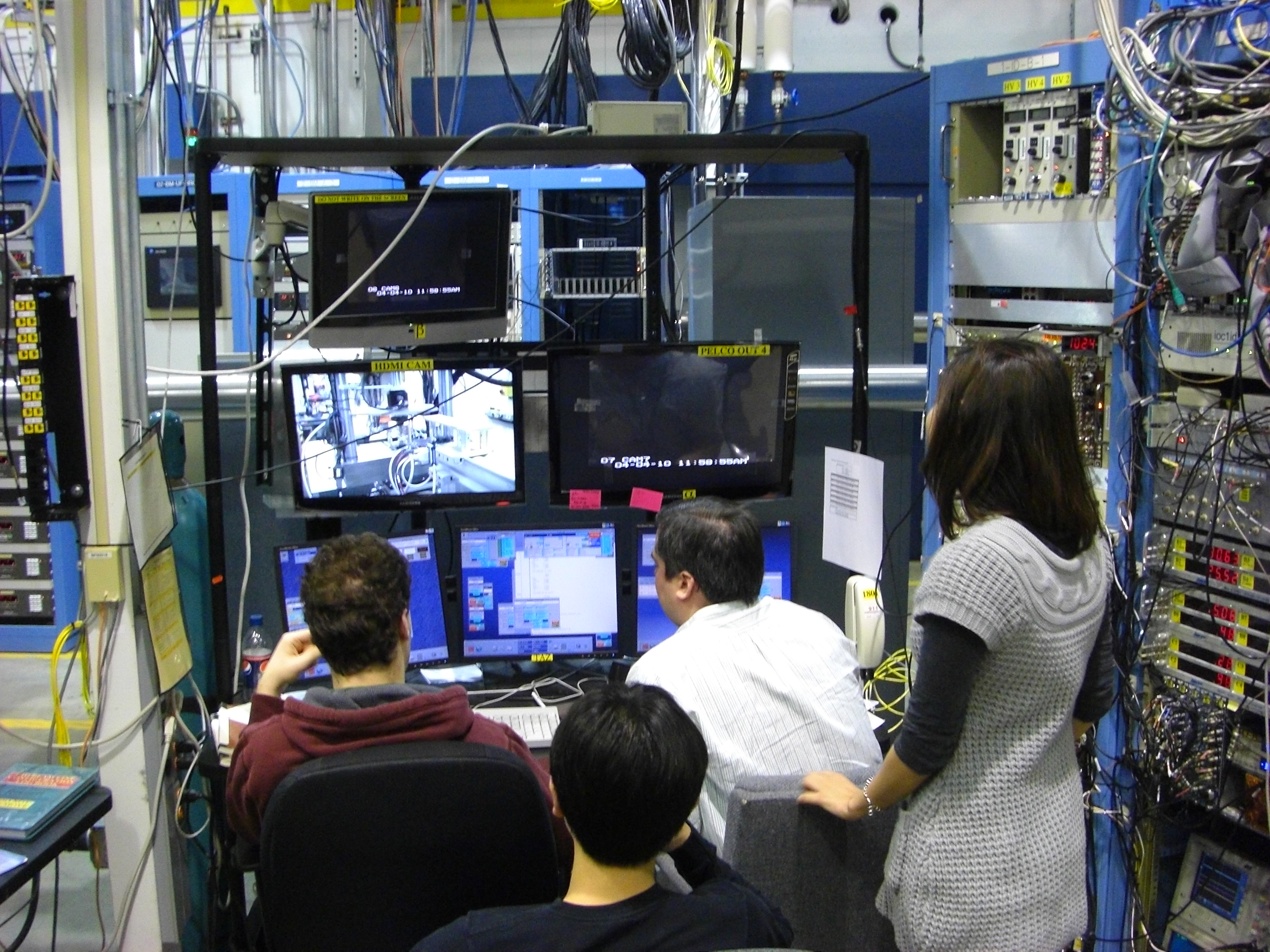
The
measurement crew (March 2010) at 1-ID command central |
Return to top
Some examples of microstructure
measurements using x-ray diffraction microscopy (updates are coming
soon...Nov 2010)
All data shown here
were collected at the Advanced Photon Source, beamline 1-ID at Argonne
National Laboratory. Participants include Chris Hefferan, Frankie Li,
Robert Suter (CMU) and Ulrich Lienert (APS). Important computational
assistance was provided by Brian Tieman of the APS; analysis was
performed using custom software developed at CMU running on a 68 node
cluster at the APS.
Questions or
comments? e-mail:
suter@andrew.cmu.edu
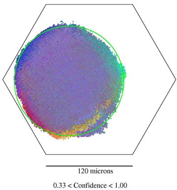
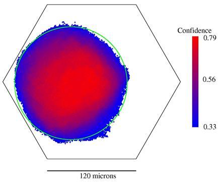
1. A section through the middle of a NIST certified 152
micron diameter single crystal ruby sphere. a) The color map on
the left shows misorientations from the average orientation.
Red-green-blue color contributions are proportional to the Rodrigues
vector describing the misorientation.
The maximum rotation angle is 0.3 degrees.
The green circle shows the nominal 152 micron sample cross-section
while the hexagon shows the entire region included in the analysis. The
maximum radial deviations are roughly 8 microns. b) The map on the
right shows the 'confidence' fitting parameter indicating maximal
overlap of the simulation with the experimental data in the central
region and reduced overlap near the edges. This reduction is due to
background subtraction removing weak edges of the imaged diffraction
spots. This fit is based on simulation of 1118 ruby Bragg peaks about
115 of which could be observed at more than one detector distance in
the experimental data set. A confidence of 0.79 means that over 90
simulated peaks overlap experimentally observed peaks; 0.33 confidence
implies 38 overlaps.
 |
 |
Ruby sphere orientation map (expanded scale)
|
Relative confidence map for image at left
|
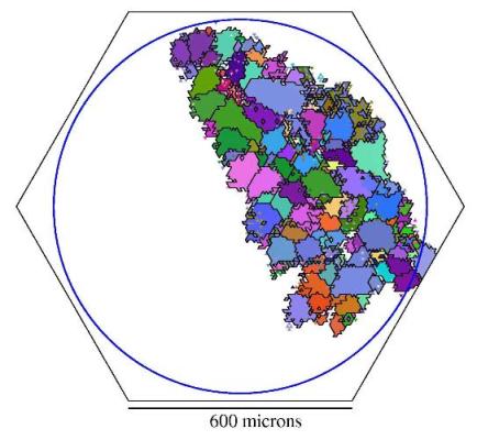
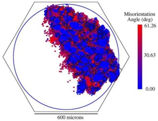
2. Near surface sections through an aluminum 1050 alloy
polycrystal sample. Colors indicate grain orientations,
again coded by Rodrigues vector components. The blue circle indicates
the 1 mm nominal sample diameter while the hexagon is the analysis box.
Black lines in the maps are draw between elements with more than 5
degree misorientation.
- Evidently, the sample surface is not parallel to the x-ray beam
nor is it planar -- in the image at right, 10 microns deeper into the
material, the fitted region has expanded on both the lower left and
upper right sides.
- The appearance of regions of apparently uniform color is the
result of many triangular area elements being independently found to
have similar crystallographic orientation. That is to say, the grain
structure emerges from the analysis -- sharp Bragg scattering is assume
to emerge from each element, but no neighbor correlations are assumed.
On expanded color scales or through quantitative analysis, one sees
that some grains contain orientation gradients corresponding to defect
content. Note that some five degree boundary lines separate regions of
almost the same color -- these are low angle grain boundaries.
- The third image below shows a map of the misorientation between
the two layer shown here. With 10 micron separation between layers,
most of the area is occupied by the same grains and has low
misorientation (blue). Since the grain boundaries are in general tilted
relative to the translation axis, there is significant misorientation
near the grain boundaries (boundaries from the z=0 layer are
superimposed).
- After measuring many such layers, a three dimensional digital
representation of the sample microstructure can be created. Since the
measurement is non-destructive, one can treat the sample in some way
(annealing, straining,...) and re-measure to see how the structure
responds.
z =
0
|
 |
| z = -10um |
|
Point-to-point crystallographic
misorientation between the above two layer measurements. Black lines
show boundaries in the z = 0 layer.
|
 |
Return to
top
Overview of relevance of HEDM microstructure mapping
techniuqe
Polycrystals are aggregates of single
crystals joined together by a network of internal interfaces called
grain boundaries. Polycrystalline materials, in both single and
multi-phase forms, are ubiquitous in engineered systems: integrated
circuits, aircraft and automotive components, communications devices,
machine tools, and many others. The three dimensional geometry,
arrangement, and relative orientation of the grains and the consequent
grain boundary network (i.e., the microstructure) are crucial
determinants of mechanical, chemical, thermal, and electrical
properties. While there has been dramatic progress made in gaining
three dimensional information about microstructure from two dimensional
measurements made at surfaces (CMU
MRSEC), it remains a great challenge to be able to watch
microstructural evolution in response to external stimuli. With such
observations made deep inside bulk materials, we should be able to
deepen our understanding of phenomena and develop accurate constitutive
relations governing the evolution and thereby learn how to do
predictive calculations and to tailor
microstructures to specific applications.
Three Dimensional X-ray Diffraction
Microscopy (see articles listed
above and the monograph by H.F. Poulsen, "Three Dimensional X-ray
Diffraction Microscopy," Springer, 2004) is the only method available
that can non-destructively image macroscopic volumes of
internal microstructures. Based simply on Bragg diffraction, it is as
versatile as, for example, electron backscatter diffraction analysis of
surface microstructures. But by using high energy x-rays, it looks
through millimeters of material without the need for destructive
serial sectioning. Similar to serial sectioning work,
measurements are done layer-by-layer. After
the measurement, the sample still exists and can be re-measured after
processing. Real-time dynamics can be monitored. The x-rays can
penetrate sample chambers, making in-situ measurements possible. In
sum, high energy x-ray diffraction microscopy (HEDM) promises to open
the world of microstructure dynamics and response to a new light. In
combination with powerful new computational tools, one can look forward
to a new level of understanding and a new level of "dynamic three
dimensional command over materials structure," (ONR BAA 04-024)
processing, and properties.
Return
to
top