Return
to Facilities Home Page
Three-Dimensional X-ray Diffraction Microscopy:
Seeing microstructure inside of bulk materials
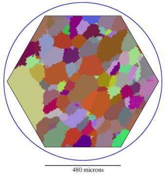
Internal layer of aluminum polycrystal measured with x-ray
diffraction microscopy at the
Advanced Photon Source (R.M. Suter,
C.M. Hefferan, S.F. Li, D.
Hennessy, C. Xiao, U. Lienert, B. Tieman, submitted ):
Colors correspond to different lattice orientations
Circle indicates 1mm nominal sample size
Hexagon indicates simulated region used in reconstruction
|
Table of Contents
- Recent publications
- Overview
- Technique summary and schematic
- Apparatus at the APS
- The July 2004 crew
Return to top
Related Publications
- Probing
Microstructure Dynamics With X-ray Diffraction Microscopy,
R.M. Suter, C.M. Hefferan, S.F. Li, D. Hennessy, C. Xiao, U. Lienert,
B. Tieman, J. Eng. Mater. Technol., 130, 021007 (2008); proceedings of
the Materials Processing
Defects-5
conference, Cornell University, July 2007).
-
3-Dimensional
Characterization of Polycrystalline Bulk Materials Using High-Energy
Synchrotron Radiation, U.
Lienert, J. Almer, B. Jakobsen, W. Pantleon, H.F. Poulsen, D. Hennessy,
C. Xiao, and R.M. Suter, Materials Science Forum 539-543, 2353-2358 (2007).
- Forward
Modeling Method for Microstructure Reconstruction Using X-ray
Diffraction
Microscopy: Single Crystal Verification, R.M. Suter, D.
Hennessy, C. Xiao, U. Lienert. Reviews
of Scientific
Instruments, 77, 123905
(2006).
-
Tracking: a
method for structural characterization of grains in powders or
polycrystals, E.M. Laurdisen, S. Schmidt, R.M. Suter, and H.F.
Poulsen, J. Appl. Cryst., 34, 744-750 (2001).
-
Three-dimensional
maps of grain boundaries and the stess state of individual grains in
polycrystals and powders, H.F. Poulsen, S.F. Nielsen, E.M.
Laurdisen, S. Schmidt, R.M. Suter, U. Lienert, L. Margulies, T.
Lorentzen, and D. Juul Jensen, J. Appl. Cryst., 34,
751-756 (2001).
- Future Trends:
Texture Analysis for Structure-Sensitive Properties, B.L. Adams, D. Juul
Jensen, H.F. Poulsen, and R. Suter, Materials Science Forum, 273-275, 29-40 (1998).
Return to top
Overview
Polycrystals are aggregates of single
crystals joined together by a network of internal interfaces called
grain boundaries. Polycrystalline materials, in both single and
multi-phase forms, are ubiquitous in engineered systems: integrated
circuits, aircraft and automotive components, communications devices,
machine tools, and many others. The three dimensional geometry,
arrangement, and relative orientation of the grains and the consequent
grain boundary network (i.e., the microstructure) are crucial
determinants of mechanical, chemical, thermal, and electrical
properties. While there has been dramatic progress made in gaining
three dimensional information about microstructure from two dimensional
measurements made at surfaces, (CMU
MRSEC) it remains a great challenge to be able to watch
microstructural evolution in response to external stimuli. With such
observations made deep inside bulk materials, we should be able to
deepen our understanding of phenomena and develop accurate constitutive
relations governing the evolution and thereby learn how to tailor
microstructures to specific applications.
Three Dimensional X-ray Diffraction
Microscopy (see articles listed
above and the monograph by H.F. Poulsen, "Three Dimensional X-ray
Diffraction Microscopy," Springer, 2004) is the only method on the
horizon that can non-destructively image macroscopic volumes of
internal microstructures. Based simply on Bragg diffraction, it is as
versatile as, for example, electron backscatter diffraction analysis of
surface microstructures. But by using high energy x-rays, it looks
through millimeters of m material. Similar to serial sectioning work,
measurements are done layer-by-layer. However, after
the measurement, the sample still exists and can be re-measured after
processing. Real-time dynamics can be monitored. The x-rays can
penetrate sample chambers, making in-situ measurements possible. In
sum, three dimensional x-ray diffraction microscopy promises to open up
the world of microstructure dynamics and response to a new light. In
combination with powerful new computational tools, one can look forward
to a new level of understanding and a new level of "dynamic three
dimensional command over materials structure," (ONR BAA 04-024)
processing, and properties.
As a part of CMU's Mesoscale Interface Mapping
Project
(MIMP) (sponsored by the NSF
MRSEC program) we are working to develop a facility for x-ray
diffraction microscopy at the Advanced
Photon Source at Argonne National
Laboratory. We are specifically working to advance the state of
non-destructive 3D microstructure mapping using high energy x-rays.
Return
to top
Schematic and Outline of the Technique
- White (multi-wavelength) synchrotron radiation from an undulator
source enters the experimental enclosure.
- Bragg diffraction from a bent single crystal of silicon (in
transmission) is used to generate a convergent monochromatic beam (50
-100keV) of x-rays.
- The line focused high energy beam (red) illuminates a ~1 micron
thick section of the sample (green).
- Bragg spots (black) from individual grains are imaged on a CCD
detector (gray); spots have the shape of the illuminated grain cross
section projected onto the detector plane at the scattering angle.
- Measuring a set of spots at multiple sample-to-detector distances
yields the path of the diffracted beam and, by inversion, the position
of
the diffracting grain.
- Step-wise measurements over a range of sample orientations, omega, yield multiple spots from
each grain; this implies complete crystallographic orientation
information and projected images of each grain from multiple points of
view.

- After image processing, our analysis code performs a simulation
of the entire measurement and microstructure. The sample space is
gridded and the crystallographic (or chemical) phase and orientation at
each grid element is adjusted to optimize the overlap
of simulated Bragg scattering with the experimental data.
Return
to top
Apparatus at APS beamline XOR-1
The following images were taken during our
July 2004 beam time:
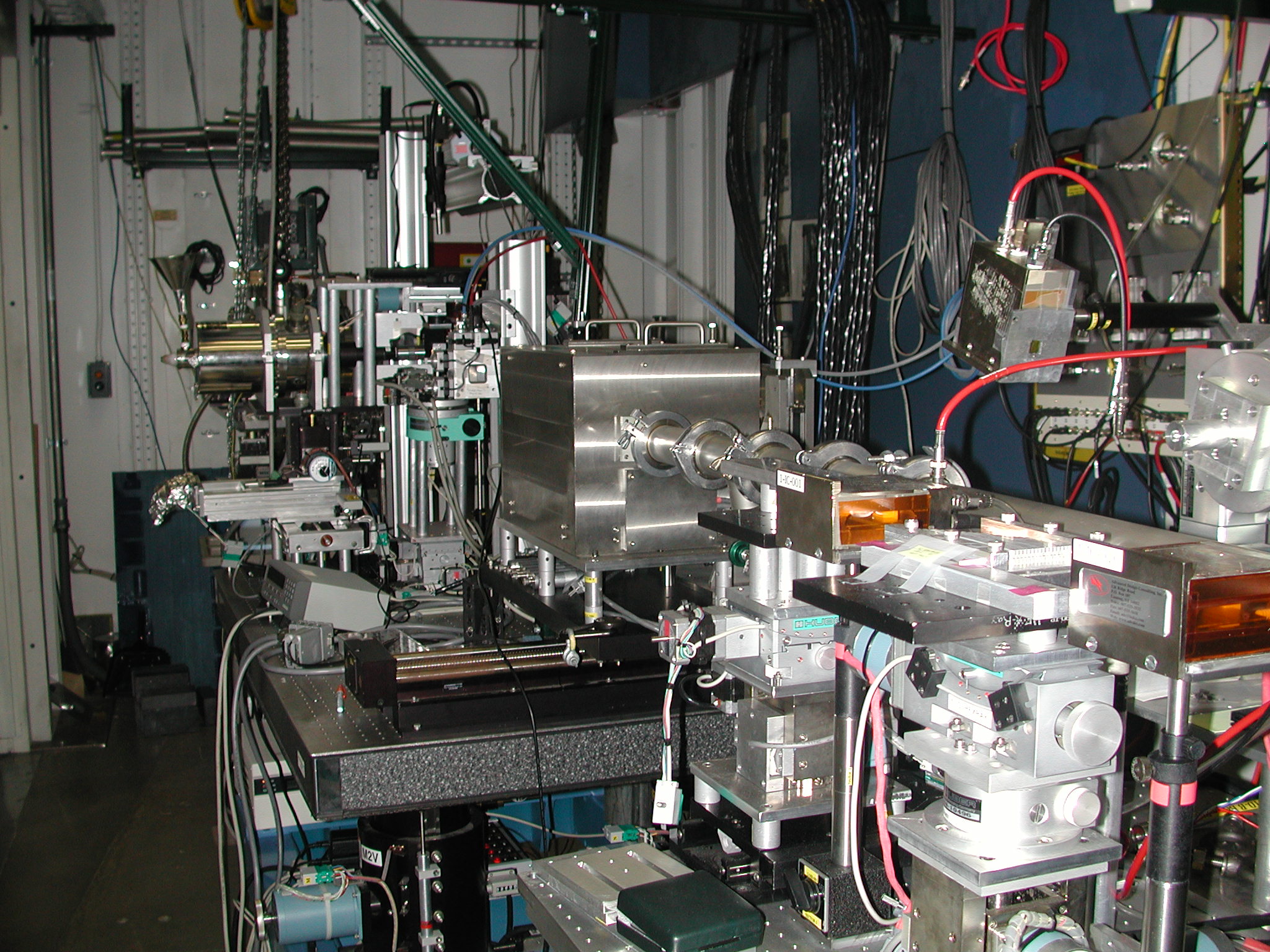
The experimental
hutch. The white beam enters from the right and travels in an evacuated
pipe into the monochromator box (roughly cubical box on optical table).
Slits before the sample (see below) reduce background and can be
used to limit the horizontal width of the line focused beam. The
sample stage and detector system follow (the horizontal stainless steel
cylinder with funnel on top is the liquid nitrogen chamber that cools
the CCD.
The heavy slits are at
right followed by an ion chamber for monitoring the incident beam
intensity (white, blue and red cables are attached). The sample
rotation (Huber green), omega, and translation stages (XY) are seen
next. The CCD lens (coming in from left) is pointing at a mirror that
directs light from an x-ray detector crystal (see below). The
entire CCD system is mounted on a translation stage so that the
sample-to-detector distance can be varied.
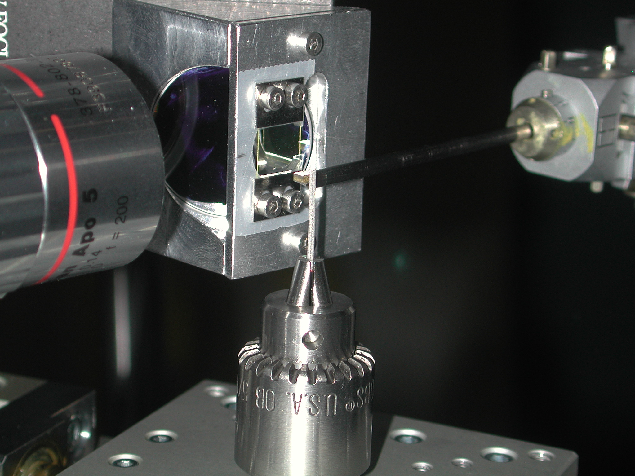
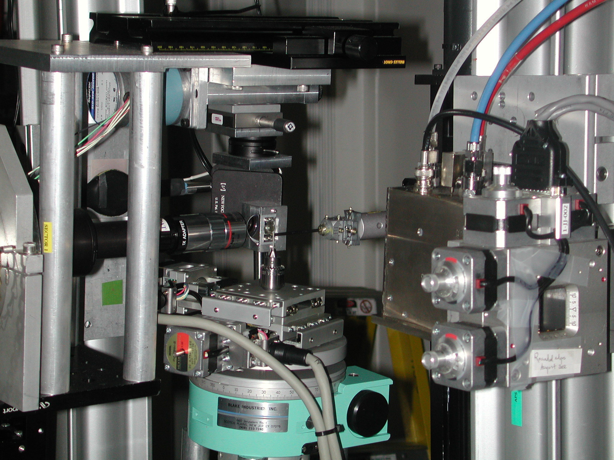
Close-up of a mounted
sample (in the drill chuck), Ta beam stop (perpendicular to sample and
mounted in a goniometer at right), transparent x-ray detector crystal
(Ce doped YAG), mirror, and lens that couples light to the CCD (out of
view to left).
Return to top