SEMITIP, VERSION 4, DOCUMENTATION
A program for computing the electric potential and tunnel current due to a probe
tip in proximity to a semiconductor, with circular symmetry. Prolate
spheroidal coordinates are used in the vacuum, and a carefully chosen
updating scheme is used to ensure stability of the iterative solution.
Includes capability for a user specified distribution of surface states.
Version 4.0 - written by R. M. Feenstra, Carnegie Mellon University,
Aug 2009
Version 4.1 - posted Dec 13, 2010
Version 4.2 - posted Jan 13, 2011
All routines are written in standard FORTRAN.
A complete description of the background theory of this
program is contained in Refs. 1-4. Some examples of running the program are provided in the
SEMITIP V4 Introduction.
Also, a user should carefully study the documentation for
VERSION 1,
VERSION 2, and
VERSION 3 of the program. The major change in VERSION 4 compared to VERSION 3 is that computations of the tunnel current are now possible. Additionally, VERSION 4 incorporates several changes to the input and output from the program, to permit upwards compatibility to VERSION 5. Specific changes in VERSION 4 compared to VERSION 3 include:
-
The number of entries in the charge density table is now user specified, line 40 of FORT.9 (in prior versions this value was set in the program to 50000).
-
In the output file FORT.10, the fourth entry is now the contact potential, rather than the opening angle of the tip shank.
-
Fort.14 and FORT.15 have been added, containing values for the tunneling current and conductance, respectively. The conductance is computed according to the value of the modulation voltage on line 19 of FORT.9, being the difference between the currents at sqrt(2)xVmod and -sqrt(2)Vmod (the modulation voltage is thus interpreted as the rms value for a lock-in amplifier).
-
Multiple input sample bias voltages can now be entered; the number of biases in listed on line 41 of FORT.9, and the full list of biases is on line 42. (The bias voltages can extended on to additional lines if needed. Also, the values can be separated by either commas or blank spaces.)
-
Computations of current are for three valence bands (light hole, heavy hole, and split-off band) and a single conduction band. All of the relevant effective masses are entered in FORT.9, on lines 12-15, along with the spin-orbit splitting on line 16.
-
Lines 22-30 of FORT.9 contains information on possible surface states, whose charge densities can be included in the computation. Either a uniform or Gaussian-distributed bands of surface states are permitted as standard input (or, with program modifications, any user specified distribution of states is allowed). Two separate distributions of surface states are permitted as input
(see the
example 3, in which Gaussian bands are used to describe intrinsic states and a uniform band is used for extrinsic states). Given the individual charge-neutrality levels of the distributions, the program searches for the overall charge-neutrality level of the combined distribution. Each specified The distribution is assumed to be uniform if the specified parameter for the Gaussian FWHM is zero. For a specified Gaussian distribution, two Gaussian bands are assumed, with the center of each band separated from the charge-neutrality level by plus or minus the centroid energy. The input densities (lines 23 and 27) now refer to the integrated densities over the band. Line 22 is a indicator of whether the temperature dependence of the surface state occupation should be included (this dependence is not included in VERSION 3 or prior versions). Including this term necessitates additional computations for determining the table of surface charge densities, prior to each voltage point computed. In most cases including this temperature dependence is not necessary, since a very similar effect can be achieved by some small shift of the parameters used to describe the surface states themselves (See
example 1 for further discussion).
-
Lines 31 of FORT.9 contains a value for the electron affinity of the semiconductor (energy difference between vacuum level and conduction band minimum). This value is needed, along with the contact potential and bias voltage, in order to construct the vacuum barrier and compute the wavefunction decay through the barrier.
-
Lines 32 of FORT.9 contain a value for the Fermi-energy of the tip, relative to the bottom of the metallic band of the tip (typically 8 eV). The theory assume that this value is relatively large, in which case there is not dependence on this value other than as a multiplier in the pre-factor for the tunneling current.
-
Lines 41-44 of FORT.9 contains values for parameters involved in the computation of the tunnel current.
Line 41 is the number of parallel wavevector values to sum over (same number of values are used for in each of kx and ky), and line 42 is the number energies in the energy integral. Line 43 refers to the step size in the integration of Schrödinger's equation performed to obtain the wavefunctions. Line 44 is the depth into the semiconductor that this integration is performed over; e.g. a value of 0.75 means that the integration extends over three-quarters of the grid points inside the semiconductor. The grid points become further and further apart as the depth into the semiconductor increases, whereas for the integration of Schrödinger's equation it is necessary to maintain some fixed (suitably small) spacing. Hence, limiting the integration such that it stops after, say, 0.5 or 0.75 of the grid points (i.e. at which point the potential is negligible) provides some saving in the computation time required.
-
Lines 48-50 of FORT.9 contain information on the V-shaped s(V) ramp used in the spectroscopic measurement. If no such ramp was used, then these parameters can all just be set to zero.
-
A PARAMETER statement at the beginning for the main program defines the array
dimensions. (This type of statement might be compiler specific, and if necessary it can easily be changed to explicit numerical array dimensions and assignment statements for the variables NRDIM, NSDIM, etc. as in VERSION 3 or earlier).
Changes to VERSION 4.1 compared to VERSION 4.0 are:
-
In VERSION 4.0, usage was made of Kane's two-band model for obtaining the decay length of the wavefunction
at energies throughout the forbidden gap region (E. O. Kane, J. Phys. Chem. Solids 1, 249 (1957)). This model describes the continuous evolution in a state from electron-character (near the conduction band edge) to hole-character (near the valence-band edge). The light-hole band is assumed to be connected in this sense to the lowest lying conduction band, whereas the heavy-hole and split-off valence bands are connected to higher lying conduction bands. See Y.-C. Chang, Phys. Rev. B 25, 605 (1982) for a description of the relevant complex band structures. Thus, in VERSION 4.0, values for the energy gaps between the heavy-hole band and its connected conduction band and betwen the split-off band and its connected conduction band were input to the program, and these values were employed in the computation of the tunnel current. The results of the computations are generally very insensitive to these two parameters, except when observable current occurs for energies deep within the band gap. That situation might occur, e.g., when probing the current very near the onset of a band edge in the presence of large band bending, in which case the two-band solution for the decay length can produce an observably different current. The two-band solution for the decay length can also play a role when inversion occurs. But, additional considerations are needed to properly model that situation; when the two-band model is used and the maximal z parameter value in line 44 of FORT.9 is too large, then the inversion current will erroneously appear in both the computations of the VB current and the CB current. Since it might be difficult for a non-expert user to correctly set the value of the maximal z parameter, in VERSION 4.1 we have eliminated usage of the two-band model. This was accomplished by commenting out lines 54-55 of the main program and lines 548, 556, 656, 664, 768, 783, 877, and 892 in intcurr.f. Inversion currents can still be computed, but they will occur only in the localized states of the relevant band, as is appropriate. The commented-out lines can be added back in if one wants to evaluate the influence of the two-band effects (but again, care must be taken in setting the value of the maximal z parameter for inversion situations for inversion situations). In that case, one would also add two lines following line 16 of FORT.9 giving two additional band gaps between the heavy-hole band and its connected conduction band and betwen the split-off band and its connected conduction band. For GaAs, the values are:
4.55      heavy hole energy gap (eV)
4.71      split-off energy gap (eV)
-
Output files FORT.91 - FORT.94 have been added, provided separately the currents and conductances from the valence band and conduction band.
Changes to VERSION 4.2 compared to VERSION 4.1 are:
-
A new grid for the z coordinates in the semiconductor has been implemented. These values, which we denote by s, are now given by:
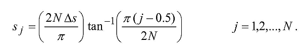 This spacing is analogous to that used for the r coordinates (as described in Ref. 2), with the first s value spaced from the surface by only one-half Δs. This smaller spacing for the first point provides an improved description of the potential near the surface, where it is varying rapidly. Regarding the value of the potential at the final value of s, it is not zero, but rather it is given by the solution to Poisson's equation employing a boundary condition that, in effect, corresponds to the Von Neumann condition (zero slope of the potential). This same condition is used at the largest r value as well.
References:
1. R. M. Feenstra, Electrostatic Potential for a Hyperbolic Probe Tip near a Semiconductor, published in J. Vac. Sci. Technol. B 21, 2080 (2003). For preprint, see
http://www.cmu.edu/physics/stm/publ/52/.
2. R. M. Feenstra, S. Gaan, G. Meyer, and K. H. Rieder, Low-temperature tunneling spectroscopy of Ge(111)c(2x8) surfaces
, Phys. Rev. B 71, 125316 (2005). For preprint, see
http://www.cmu.edu/physics/stm/publ/65/.
3. R. M. Feenstra, Y. Dong, M. P. Semtsiv, and W. T. Masselink, Influence of Tip-induced Band Bending on Tunneling Spectra of Semiconductor Surfaces, Nanotechnology 18, 044015 (2007). For preprint, see
http://www.cmu.edu/physics/stm/publ/74/.
4. Y. Dong, R. M. Feenstra, M. P. Semtsiv and W. T. Masselink, Band Offsets of InGaP/GaAs Heterojunctions by Scanning Tunneling Spectroscopy, J. Appl. Phys. 103, 073704 (2008).
For preprint, see
http://www.cmu.edu/physics/stm/publ/79/.