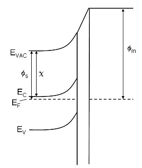
The contact potential, Δφ (measured in unit of energy, eV), is one of the most important parameters for understanding tip-induced band bending and tunneling spectroscopy. It is defined as the work function of the metallic tip, φm, minus that of the semiconducting sample, φs, where for the sample its work function is given by the electron affinity, χ, plus the difference in energy between the conduction band maximum and the Fermi-level, EC-EF. For the contact potential used throughout the SEMITIP program, it is assumed that we are taking the work function of the sample as it would be in the absence of any surface states (intrinsic or extrinsic). Such surface states can still be included in the program with no problem, but it's just that the contact potential, as a numerical parameter, corresponds to what would be measured experimentally on a surface with no surface states.
If, for example, a positive contact potential occurs, then, when a tip is brought towards a sample, upwards band bending will occur in the sample. The situation for an n-type sample is pictured below, with the surface region being depleted of electrons. It is clear that a nonzero electrostatic potential exists in the semiconductor, even though there is not applied voltage bias between the sample and tip.
In the above diagram, it is clear that the electrostatic potential energy within the probe tip, relative to a point deep inside the semiconductor, is given simply by Δφ. Application of some bias voltage Von the sample relative to the tip will further shift the electrostatic potential energy of the tip by eV (e is the fundamental unit of charge, taken as usual to be positive), so that the total electrostatic potential energy of the tip is φT=eV+Δφ as defined in Ref. 1. This quantity is the basic boundary condition used for the electrostatic solution within SEMITIP. In versions 1 and 2 is was φT itself that was entered as an input parameter. In version 3 and higher, separate parameters for V and Δφ are entered. (In version 3 these parameters are used simply to compute the sum eV+Δφ, which is assigned to φT, whereas in versions 4 and higher, where tunnel currents are computed, the quantities V and Δφ are needed individually for other purposes as well).
References:
1. R. M. Feenstra, Y. Dong, M. P. Semtsiv, and W. T. Masselink, Influence of Tip-induced Band Bending on Tunneling Spectra of Semiconductor Surfaces, Nanotechnology 18, 044015 (2007). For preprint, see
http://www.cmu.edu/physics/stm/publ/74/.